Published by: BhumiRaj Timalsina
Published date: 26 Jun 2021
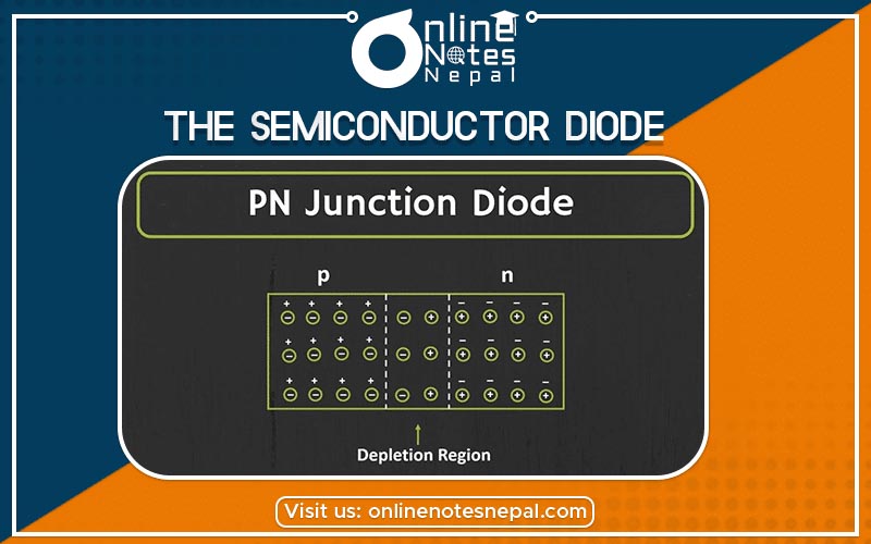
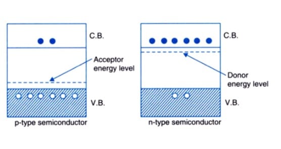
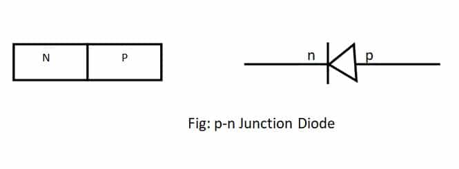
The Semiconductor Diode is a device that permits the current flow in only one direction. It is also called the P-N Junction diode. It consists of a p-type semiconductor placed in contact with the n-type semiconductor. Together, they form a p-n junction where the n layer with electron donor dopants has an excess amount of electrons. These are the majority carriers there. We have more electrons here than the holes. However, in the ‘p’ layer (electron acceptor dopants) the majority carriers are electron holes rather than electrons. So, we have more holes to fill, than electrons available. The electron-hole is vacant. Travelling of the electron from its initial place to other location inside the crystal creates this.
We can neutralize the electrons and holes by the positive space change ions and negative space ions respectively. When the two types of semiconductors come in contact with each other, there will be a net diffusion of electrons from the n-region into the p-region. When it crosses the junction, these electrons reach in a region where there are lot of holes to recombine with. The holes in the p-junction diffuse across the junction into the n-region and can combine with the electrons. At the same time, the immobile donor ions on the ‘n’ side and acceptor ions on the ‘p’ side are in charge condition. These charged layers on each side of the junctions create an internal electric field that prevents further diffusion.
 Thus, there is an establishment of equilibrium. There is no net current across the junction. The charge layer creates a potential difference Vc between both sides of the junction. The n-side which is the positively charged will be at the higher potential than the p-side, which is negatively charged. When an electron is in the n-region its potential energy is Ep = -I e I Vc. Whereas, in the p-region, the potential energy is Ep = 0. It means the potential energy of the electron is shifted upward relative to the n side by an amount I e I Vc. These potential energy barriers stop the further flow of majority carriers across the junction.
One of the consequences of the contact potential is the upward shift of the electronic energy bands in the p-side, relative to the bands in the side by an amount I e I Vc. The energy band of the n-type and p-type semiconductor before contact is in the figure below: