In an integrated circuit, electronic components such as resistors, capacitors, diodes, and transistors are formed directly onto the surface of a silicon crystal. IC Manufacturing as a process entails quite a number of specific steps, which are necessary to ensure the high production of quality microchips.
The IC manufacturing process can be summarised briefly. It all starts with a suitable semiconductor material, such as silicon. It is refined to a highly pure state and then sliced into thin sheets. From these sheets, a photoresist film is added to imprint the circuitry as it bakes and is then etched to create a permanent configuration. The Si wafer is then doped with specialized impurities. As mentioned, multiple layers can be etched onto a single IC chip. The chips are then tested, separated and packaged, ready for delivery.
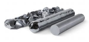
Purification
Silicon is found in quartzite
The second most abundant element behind oxygen
Other elements must be removed
Quartzite heated to 2000⁰C then purified again through a chemical process
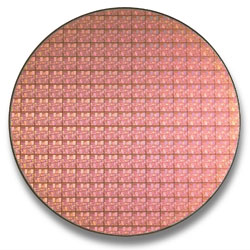
Silicon is now in rod form and sawed into wafers
Fig: Silicon Wafer
Wafer Preparation
The wafer is polished to be almost mirror-like
The final chemical process removes polishing materials
Wafers packaged in the ultra‐clean facility and ready for the fabrication process
Semiconductor Fabrication Plant
Built to keep dust particles off of semiconductors, to dampen vibrations, and to control humidity and temperature
Hundreds of pieces of equipment are needed
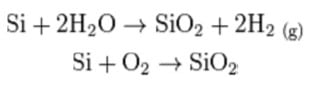
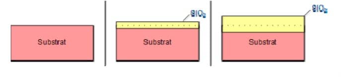
Thermal Oxidation
Usually performed at a temperature between 800 and1200ºC, creating a High-Temperature Oxide layer
May use either water vapor or molecular oxygen as the oxidant (called either wet or dry oxidation).
Dry Oxidation: slow growth of oxide, high density, high breakdown voltage.
Wet Oxidation: fast growth (even on low temperatures), less quality than dry oxides.
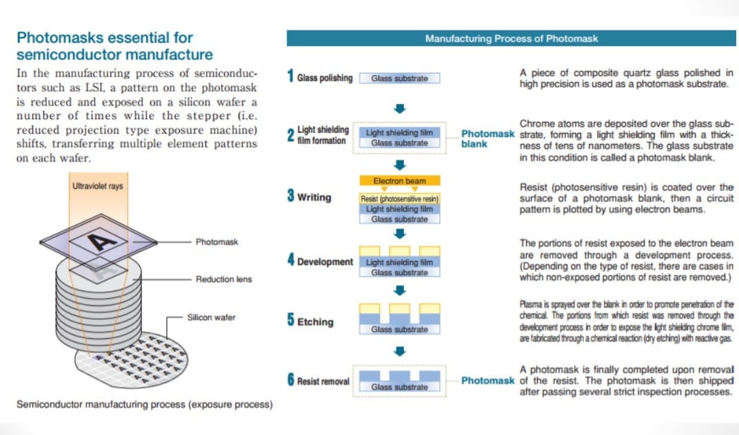
Photomasking
Etching Process
The semi‐conductor covered in ‘masking material’ (photoresist)
The etching forms cavities in semi‐conductor layers according to design.
The goal is to completely remove one layer, without harming the underlying layer.
Three main types of etching: Wet, Dry, Plasma
Plasma Etching
Uses ions of gases, mainly Argon
Shoots ions toward the layered surface
Transfer of momentum creates the desired cavity
Diffusion Process
Pure silicon doped with specific types of atoms
Alters electrical properties, mainly conductivity
Allows one to determine the carrier concentration
Atoms used for doping:
Group III (boron)‐ produce p‐type semiconductor
Group V (phosphorous)‐ produce n‐type semiconductor
Heated to extreme temperatures to ‘diffuse’ with intrinsic silicon
Ion Implantation
Process of shooting ions of the desired dopant species into the wafer through openings in the oxide or photoresist.
Low-temperature technique.
It provides flexibility not available with diffusion.
Ion Implanter is a large complex and expensive piece of equipment. It’s made of several vacuum systems and a computer-controlled electronic system.
Metallization, Bonding, and Packaging
Metallization is a specialized deposition process that forms critical interconnections between different areas of the chip and different transistors.
Also used to form the bonding pads that connect the chip to package and then to the circuit board of the system it supports.
Wire Bonding is used to connect the bonding pads on the die to the post (bonding area). There are three types of bonding: Thermo compression, ultrasonic, and thermo sonic ball bonding.
The packaging is completed by sealing the pieces of the housing together or by encapsulation with a molding component.