
Published by: BhumiRaj Timalsina
Published date: 30 Jun 2021
Clock circuits are the circuits that produce periodic pulses. Most sequential circuits are drive by a clock circuit. A clock signal is a particular type of signal that oscillates between a high and a low state. A clock can be constructed with a multivibrator.
Some of the clock generators are discussed below:
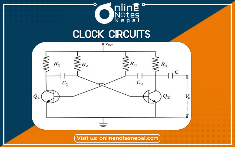
An astable multivibrator has no stable states. Once the Multivibrator is ON, it just changes its states on its own after a certain time period which is determined by the RC time constants. A dc power supply or Vcc is given to the circuit for its operation.
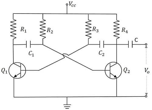
Fig: Astable Multivibrator
When Vcc is applied, the collector current of the transistors increases. As the collector current depends upon the base current,
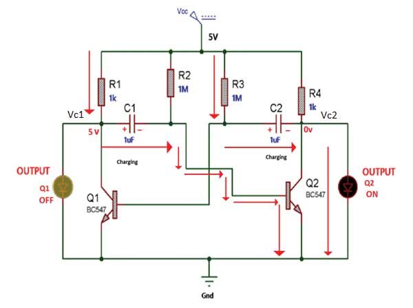
As no transistor characteristics are alike, one of the two transistors says Q1 has its collector current increase and thus conducts. The collector of Q1 is applied to the base of Q2 through C1. This connection lets the increased negative voltage at the collector of Q1 to get applied at the base of Q2 and its collector current decreases. This continuous action makes the collector current of Q2 to decrease further. This current when applied to the base of Q1 makes it more negative and with the cumulative actions, Q1 gets into saturation and Q2 to cut off. Thus the output voltage of Q1 will be VCE (sat) and Q2 will be equal to VCC.
The capacitor C1 charges through R1 and when the voltage across C1 reaches 0.7v, this is enough to turn the transistor Q2 to saturation. As this voltage is applied to the base of Q2, it gets into saturation, decreasing its collector current. This reduction of voltage at point B is applied to the base of transistor Q1 through C2 which makes the Q1 reverse bias. A series of these actions turn the transistor Q1 to cut off and transistor Q2 to saturation. Now point A has the potential VCC. The capacitor C2 charges through R2. The voltage across this capacitor C2 when it gets to 0.7v turns on the transistor Q1 to saturation.
Hence the output voltage and the output waveform are formed by the alternate switching of the transistors Q1 and Q2. The time period of these ON/OFF states depends upon the values of biasing resistors and capacitors used, i.e., on the RC values used. As both the transistors are operated alternately, the output is a square waveform, with the peak amplitude of VCC.
The output taken from the collector of either transistor is shown in the graph.
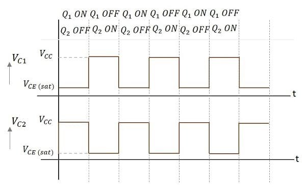
The ON time of transistor Q1 or the OFF time of transistor Q2 is given by
t1 = 0.69R1C1
Similarly, the OFF time of transistor Q1 or ON time of transistor Q2 is given by
t2 = 0.69R2C2
Hence, the total time period of the square wave
t = t1 + t2 = 0.69(R1C1 + R2C2)
As R1 = R2 = R and C1 = C2 = C, the frequency of square wave will be
A circuit called the free-running oscillator clock made with two inverters is shown in the figure:
Suppose that initially VA=OV, then, VB will be 5V and VD=0V
The capacitor C will begin to charge. This charging will continue until the voltage at A has risen sufficiently to cause the voltage at B becomes OV and hence VD=5V.
Now, the capacitor will now discharge until the voltage at A sufficiently enough to cause the voltage at B becomes 5V and consequently VD=DV.
The values of R and C determine the cycle of the clock.