Published by: Nuru
Published date: 22 Jun 2021

The design of combinational circuits starts from the verbal outline of the problem and ends in a logic circuit diagram or a set of Boolean functions from which the logic diagram can be easily obtained. The design procedure involves the following steps:
1. Specification
2. Formulation
3. Optimization
4. Technology Mapping
5. Verification
In simple words, we can list out the design procedure of combinational circuits as:
1. The problem is stated.
2. The number of available input variables and required output variables is determined.
3. The input and output variables are assigned letter symbols.
4. The truth table that defines the required relationships between inputs and outputs is derived.
5. The simplified Boolean function for each output is obtained.
6. The logic diagram is drawn.
7. Verify the correctness of the design.

Q. Design a combinational circuit with three inputs and one output. The output must be logic 1 when the binary value of the inputs is less than 110 and logic 0 otherwise. Use only NAND gates.
Input: 3 (let x, y and z)
Output: 1 (let F)
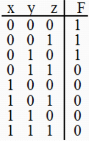
Truth Table:

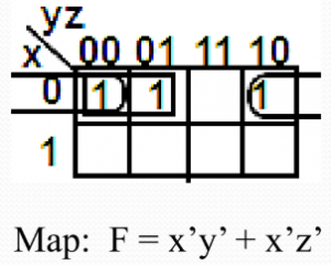
Simplification:

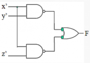
Logic Diagram:

This is a simple example of designing a combinational logic. We can design other combinational logics in similar ways.