Published by: Nuru
Published date: 22 Jun 2021

The availability of a large variety of codes for the same discrete elements of information results in the use of different codes by different digital systems. It is sometimes necessary to use the output of one system as the input to another. A conversion circuit must be inserted
between the two systems if each uses different codes for the same information. Thus, a code conversion is done to make the two systems compatible even though each uses a different binary code. To convert from binary code A to binary code B, the code converter has
input lines supplying the bit combination of elements as specified by code A and the output lines of the converter generating the corresponding bit combination of code B.
A Code converter (combinational circuit) performs this transformation by means of logic gates. The design procedure of code converters will be illustrated by means of a specific example of conversion from the BCD to the excess-3 code.
The excess-3 code for a decimal digit is the binary combination corresponding to the decimal digit plus 3.
For example, the excess-3 code for decimal digit 5 is the binary combination for 5 + 3 = 8, which is 1000.
5-step design procedure of this code converter
1. Specification
2. Formulation
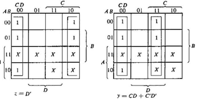
| Input BCD | Output Excess-3 code | ||||||
|---|---|---|---|---|---|---|---|
| A | B | C | D | W | X | Y | Z |
| 0 | 0 | 0 | 0 | 0 | 0 | 1 | 1 |
| 0 | 0 | 0 | 1 | 0 | 1 | 0 | 0 |
| 0 | 0 | 1 | 0 | 0 | 1 | 0 | 1 |
| 0 | 1 | 1 | 0 | 1 | 1 | 0 | 0 |
| 0 | 1 | 0 | 0 | 0 | 1 | 1 | 1 |
| 0 | 1 | 0 | 1 | 1 | 0 | 0 | 0 |
| 0 | 1 | 1 | 0 | 1 | 0 | 0 | 1 |
| 0 | 1 | 1 | 1 | 1 | 0 | 1 | 0 |
| 1 | 0 | 0 | 0 | 1 | 0 | 1 | 1 |
| 1 | 0 | 0 | 1 | 1 | 1 | 0 | 0 |
Note that the four BCD input variables may have 16-bit combinations, but only 10 are listed in the truth table. Others designate “don’t care conditions”.
3. Optimization
a. 2-level optimization
The k-maps are plotted to obtain simplified sum-of-products Boolean expressions for the outputs. Each of the four maps represents one of the outputs of the circuit as a function of the four inputs.

b. Multiple-level optimization
This second optimization step reduces the number of gate inputs. The following manipulation illustrates optimization with multiple-output circuits implemented with three levels of gates:
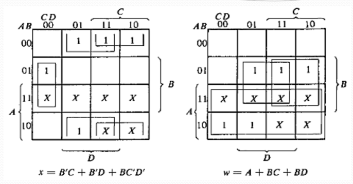
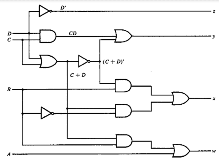
Fig: Logic Diagram of BCD- to-Excess-3 Code Converter
4. Technology mapping
This is concerned with the act of mapping of the basic circuit (using AND, OR, and NOT gates) to a specific circuit technology (such as NAND,
NOR gate tech.)