Published by: Dikshya
Published date: 10 Jul 2023

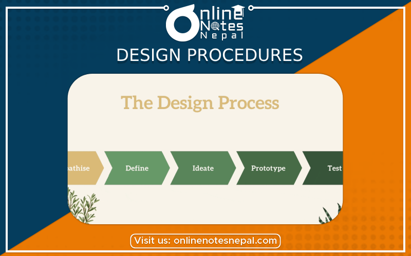
Design procedures for digital logic circuits involve a systematic approach to designing and implementing circuits. Here are the key steps typically followed in the design process:
1. Define Requirements: Clearly define the functional and performance requirements of the digital logic circuit. Understand the desired inputs, outputs, functionality, timing constraints, and any specific design constraints.
2. Specification and Analysis: Create a detailed specification of the circuit, including truth tables, state diagrams, or Boolean expressions. Perform an analysis of the desired logic function to determine the necessary gates and components.
3. Gate-Level Design: Implement the logic function using basic logic gates such as AND, OR, NOT, or XOR gates. Determine the gate-level representation of the circuit, including the interconnections between the gates.
4. Circuit Simulation: Simulate the circuit design using specialized software tools or hardware description languages (HDLs) like Verilog or VHDL. Perform functional and timing simulations to verify the correct behavior of the circuit.
5. Logic Optimization: Analyze the circuit for potential optimizations. Use techniques like logic minimization, Boolean algebra simplification, or Karnaugh maps to minimize the number of gates, reduce complexity, or improve performance.
6. Component Selection: Choose specific components based on the required functionality, performance, and constraints. Select the appropriate integrated circuits (ICs), such as MSI or LSI devices, to implement the circuit efficiently.
7. Schematic Capture: Create a detailed schematic diagram of the circuit, showing the connections between the components. Use specialized design software or computer-aided design (CAD) tools to capture the schematic representation.
8. Printed Circuit Board (PCB) Layout: If necessary, design the layout of the printed circuit board (PCB) that will hold the circuit components. Place the components, route the interconnections, and consider factors like signal integrity, power distribution, and noise reduction.
9. Prototype and Testing: Build a physical prototype of the circuit based on the schematic and PCB layout. Perform testing and validation to ensure that the circuit functions correctly and meets the specified requirements. Debug any issues and make necessary adjustments.
10. Documentation and Revision Control: Maintain proper documentation throughout the design process, including specifications, schematics, PCB layouts, and testing results. Implement revision control to track design changes and ensure version control.
Throughout the design process, collaboration, communication, and iteration are important. Regular reviews and feedback from peers or stakeholders can help refine the design and ensure its correctness.