
Published by: Nuru
Published date: 18 Jun 2021
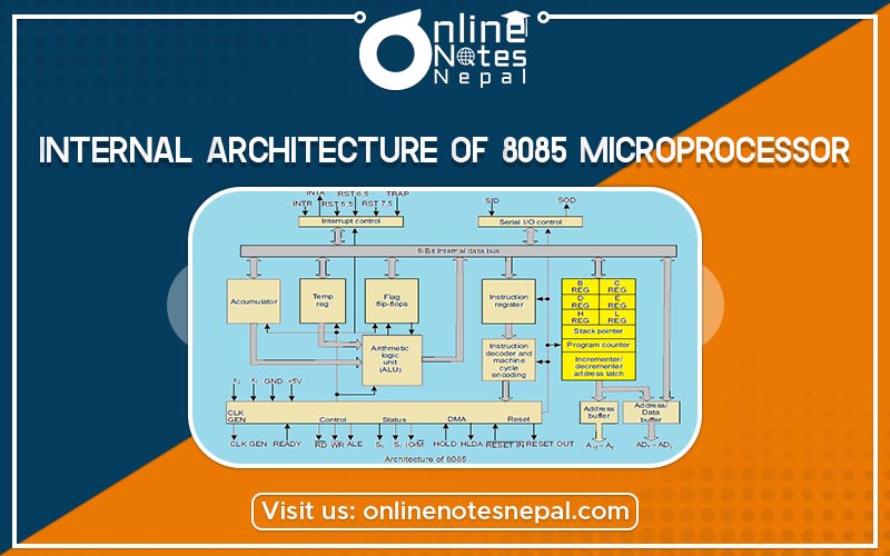
The Intel 8085 A is a complete 8-bit parallel central processing unit. The main components of 8085A are an array of registers, the arithmetic logic unit, the encoder/decoder, and timing and control circuits linked by an internal data bus. The block diagram is shown below:
1: ALU:- The arithmetic logic unit performs the computing functions, it includes the
accumulator, the temporary register, the arithmetic and logic circuits, and five flags. The
temporary register is used to hold data during an arithmetic/logic operation. The result is
stored in the accumulator; the flags (flip-flops) are set or reset according to the result of the
operation.
2. Accumulator (register A): It is an 8 bit register that is the part of ALU. This register is used to
store the 8-bit data and to perform arithmetic and logic operations and 8085 microprocessor is
called accumulator based microprocessor. When data is read from input port, it first moved to
accumulator and when data is sent to output port, it must be first placed in accumulator.
3. Temporary registers(W & Z): They are 8 bit registers not accessible to the programmer.
During program execution, 8085A places the data into it for a brief period.
4. Instruction register(IR): It is a 8 bit register not accessible to the programmer. It receives the
operation codes of instruction from internal data bus and passes to the instruction decoder
which decodes so that microprocessor knows which type of operation is to be performed.
5. Register Array: (Scratch pad registers B, C, D, E): It is a 8 bit register accessible to the
programmers. Data can be stored upon it during program execution. These can be used
individually as 8-bit registers or in pair BC, DE as 16 bit registers. The data can be directly added
or transferred from one to another. Their contents may be incremented or decremented and
combined logically with the content of the accumulator.
Register H & L: - They are 8 bit registers that can be used in same manner as scratch pad
registers.
Stack Pointer (SP): - It is a 16 bit register used as a memory pointer. It points to a memory
location in R/W memory, called the stack. The beginning of the stack is defined by loading a 16-
bit address in the stack pointer.
Program Counter (PC): - Microprocessor uses the PC register to sequence the execution of the
instructions. The function of PC is to point to the memory address from which the next byte is
to be fetched. When a byte is being fetched, the PC is incremented by one to point to the next
memory location.
The features of 8085 Microprocessor include :
1.It is an 8-bit microprocessor i.e. it can accept, process, or provide 8-bit data simultaneously.
2.It operates on a single +5V power supply connected at Vcc; power supply ground is connected to Vss.
3.It operates on clock cycle with 50% duty cycle.
4.It has on chip clock generator. This internal clock generator requires tuned circuit like LC, RC or crystal. The internal clock generator divides oscillator frequency by 2 and generates clock signal, which can be used for synchronizing external devices.
5.It can operate with a 3 MHz clock frequency. The 8085A-2 version can operate at the maximum frequency of 5 MHz.
6.It has 16 address lines, hence it can access (216) 64 Kbytes of memory.
7.It provides 8 bit I/O addresses to access (28 ) 256 I/O ports.
8.In 8085, the lower 8-bit address bus (A0 -A7) and data bus (D0 -D7) are Multiplexed to reduce number of external pins. But due to this, external hardware (latch) is required to separate address lines and data lines.
9.It supports 74 instructions with the following addressing modes :
a) Immediate
b) Register
c) Direct
d) Indirect
e) Implied
10.The Arithmetic Logic Unit (ALU) of 8085 performs:
(a)8 bit binary addition with or without carry
(b)16 bit binary addition
(c)2 digit BCD addition.
d)8-bit binary subtraction with or without borrow
(e)8-bit logical AND, OR, EX-OR, complement (NOT), and bit shift operations.
Bus is defined as a set of physical connections (Cables, Printed circuits, etc.), which can be shared by multiple hardware components in order to communicate with one another.
All computers have three fundamental buses: Control, Instruction and Address bus.
Control Bus: The motherboard's control bus manages the activity in the system. The control bus, like the other buses, is simply a set of connections among the parts in the computer.
Data Bus: The data bus acts as a conduit for data from the keyboard, memory and other devices. It passes information at speeds up to billions of characters per second. The central processor reads the data, performs calculations, and moves new data back to memory, the hard drive and other locations.
Address Bus: The computer must be able to access every character of memory rapidly, so every character has its own address number. The central processor specifies which addresses it wants to read or write and the address bus carries this information to a memory controller circuit, which locates and fetches the information.
Some of the common components of a microprocessor are:
Control Unit
I/O Units
Arithmetic Logic Unit (ALU)
Registers
Cache
A brief introduction to these components is placed below:
Control Unit
The control unit, as described above, reads the instructions, and generates the necessary digital signals to operate the other components. An instruction to add two numbers together would cause the Control Unit to activate the addition module, for instance.
I/O Units
The processor needs to be able to communicate with the rest of the computer system. This communication occurs through the I/O ports. The I/O ports will interface with the system memory (RAM), and also the other peripherals of a computer.
Arithmetic Logic Unit
The Arithmetic Logic Unit, or ALU is the part of the microprocessor that performs arithmetic operations. ALUs can typically add, subtract, divide, multiply, and perform logical operations of two numbers (and, or, nor, not, etc).
Registers
This book includes data about different kinds of registers. Hopefully it will be obvious which kind of register we are talking about from the context. The most general meaning is a "hardware register": anything that can be used to store bits of information, in a way that all the bits of the register can be written to or read out simultaneously. Since registers outside of a CPU are also outside the scope of the book, this book will only discuss processor registers, which are hardware registers that happen to be inside a CPU. But usually we will refer to a more specific kind of register.
Cache
Most CPUs manufactured do not have any cache. Cache is memory that is located on the chip, but that is not considered registers. The cache is used because reading external memory is very slow (compared to the speed of the processor), and reading a local cache is much faster. In modern processors, the cache can take up as much as 50% or more of the total area of the chip.
Arithmetic Instructions are the instructions that perform basic arithmetic operations such as addition, subtraction, and a few more. In the 8085 microprocessor, the destination operand is generally the accumulator. In the 8085 microprocessor, the destination operand is generally the accumulator. The arithmetic instructions define the set of operations performed by the processor Arithmetic Logic Unit (ALU). The arithmetic instructions are further classified into binary, decimal, logical, shift/rotate, and bit/byte manipulation instructions.