
Published by: Zaya
Published date: 26 Jun 2021
A diode made of semiconductor components, usually silicon. The cathode, which is negatively charged and has an excess of electrons, is placed adjacent to the anode, which has an inherently positive charge, carrying an excess of holes. At this junction a depletion region forms, with neither holes nor electrons. A positive voltage at the anode makes the depletion region small, and current flows; a negative voltage at the anode makes the depletion region large, preventing current flow.
A diode is a two-terminal electronic component that conducts current primarily in one direction (asymmetric conductance); it has low (ideally zero) resistance in one direction, and high (ideally infinite) resistance in the other. A diode vacuum tube or thermionic diode is a vacuum tube with two electrodes, a heated cathode, and a plate, in which electrons can flow in only one direction, from cathode to plate. A semiconductor diode, the most commonly used type today, is a crystalline piece of semiconductor material with a p–n junction connected to two electrical terminals. Semiconductor diodes were the first semiconductor electronic devices. The discovery of asymmetric electrical conduction across the contact between a crystalline mineral and a metal was made by German physicist Ferdinand Braun in 1874. Today, most diodes are made of silicon, but other materials such as gallium arsenide and germanium are also used.
The most common function of a diode is to allow an electric current to pass in one direction (called the diode’s forward direction) while blocking it in the opposite direction (the reverse direction). As such, the diode can be viewed as an electronic version of a check valve. This unidirectional behaviour is called rectification and is used to convert alternating current (ac) to direct current (dc). Forms of rectifiers, diodes can be used for such tasks as extracting modulation from radio signals in radio receivers.
However, diodes can have more complicated behaviour than this simple on-off action, because of their nonlinear current-voltage characteristics. Semiconductor diodes begin conducting electricity only if a certain threshold voltage or cut-in voltage is present in the forward direction (a state in which the diode is said to be forward-biased). The voltage drop across a forward-biased diode varies only a little with the current, and is a function of temperature; this effect can be used as a temperature sensor or as a voltage reference. Also, diodes’ high resistance to current flowing in the reverse direction suddenly drops to a low resistance when the reverse voltage across the diode reaches a value called the breakdown voltage.
A semiconductor diode’s current-voltage characteristic can be tailored by selecting the semiconductor materials and the doping impurities introduced into the materials during manufacture. These techniques are used to create special-purpose diodes that perform many different functions. For example, diodes are used to regulate voltage (Zener diodes), to protect circuits from high voltage surges (avalanche diodes), to electronically tune radio and TV receivers (varactor diodes), to generate radio-frequency oscillations (tunnel diodes, Gunn diodes, IMPATT diodes), and to produce light (light-emitting diodes). Tunnel, Gunn and IMPATT diodes exhibit negative resistance, which is useful in microwave and switching circuits. Diodes, both vacuum, and semiconductor can be used as shot-noise generators.
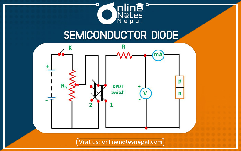
A PN-junction diode is formed when a p-type semiconductor is fused to an n-type semiconductor creating a potential barrier voltage across the diode junction
The effect described in the previous tutorial is achieved without any external voltage being applied to the actual PN junction resulting in the junction being in a state of equilibrium.
However, if we were to make electrical connections at the ends of both the N-type and the P-type materials and then connect them to a battery source, an additional energy source now exists to overcome the potential barrier.
The effect of adding this additional energy source results in the free electrons being able to cross the depletion region from one side to the other. The behaviour of the PN junction with regards to the potential barrier’s width produces an asymmetrical conducting two-terminal device, better known as the PN Junction Diode.
A PN Junction Diode is one of the simplest semiconductor devices around, and it has the characteristic of passing current in only one direction only. However, unlike a resistor, a diode does not behave linearly with respect to the applied voltage as the diode has an exponential current-voltage ( I-V ) relationship and therefore we can not describe its operation by simply using an equation such as Ohm’s law.
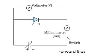
If a suitable positive voltage (forward bias) is applied between the two ends of the PN junction, it can supply free electrons and holes with the extra energy they require to cross the junction as the width of the depletion layer around the PN junction is decreased.
By applying a negative voltage (reverse bias) results in the free charges being pulled away from the junction resulting in the depletion layer width being increased. This has the effect of increasing or decreasing the effective resistance of the junction itself allowing or blocking current flow through the diode.