
Published by: Zaya
Published date: 24 Jun 2021
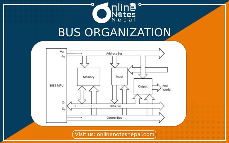
Bus is a group of conducting wires which carries information, all the peripherals are connected to the microprocessor through Bus.
Harvard Architecture
Harvard architecture has separate data and instruction busses, allowing transfers to be performed simultaneously on both busses. A Von Neumann architecture has only one bus which is used for both data transfers and instruction fetches, and therefore data transfers and instruction fetches must be scheduled - they can not be performed at the same time.
It is possible to have two separate memory systems for Harvard architecture. As long as data and instructions can be fed in at the same time, then it doesn't matter whether it comes from a cache or memory. But there are problems with this. Compilers generally embed data (literal pools) within the code, and it is often also necessary to be able to write to the instruction memory space, for example in the case of self-modifying code, or, if a debugger is used, to set software breakpoints in memory. If there are two completely separate, isolated memory systems, this is not possible. There must be some kind of bridge between the memory systems to allow this.
Using a simple, unified memory system together with a Harvard architecture is highly
inefficient. Unless it is possible to feed data into both busses at the same time, it might be
better to use a von Neumann architecture processor.
Use of caches:
At higher clock speeds, caches are useful as the memory speed is proportionally slower. Harvard architectures tend to be targeted at higher performance systems, and so caches are nearly always used in such systems.
Von Neumann architectures usually have a single unified cache, which stores both instructions and data. The proportion of each in the cache is variable, which may be a good thing. It would in principle be possible to have separate instruction and data caches, storing data and instructions separately. This probably would not be very useful as it would only be possible to ever access one cache at a time.
Caches for Harvard architectures are very useful. Such a system would have separate caches for each bus. Trying to use a shared cache on a Harvard architecture would be very inefficient since then only one bus can be fed at a time. Having two caches means it is possible to feed both buses simultaneously....exactly what is necessary for Harvard architecture.
This also allows having a very simple unified memory system, using the same address space for both instructions and data. This gets around the problem of literal pools and self-modifying code. What it does mean, however, is that when starting with empty caches, it is necessary to fetch instructions and data from the single memory system, at the same time. Obviously, two memory accesses are needed therefore before the core has all the data needed. This performance will be no better than a von Neumann architecture. However, as the caches fill up, it is much more likely that the instruction or data value has already been cached, and so only one of the two has to be fetched from memory. The other can be supplied directly from the cache with no additional delay. The best performance is achieved when both instructions and data are supplied by the caches, with no need to access external memory at all.
This is the most sensible compromise and the architecture used by certain Harvard processor cores. Two separate memory systems can perform better but would be difficult to implement.
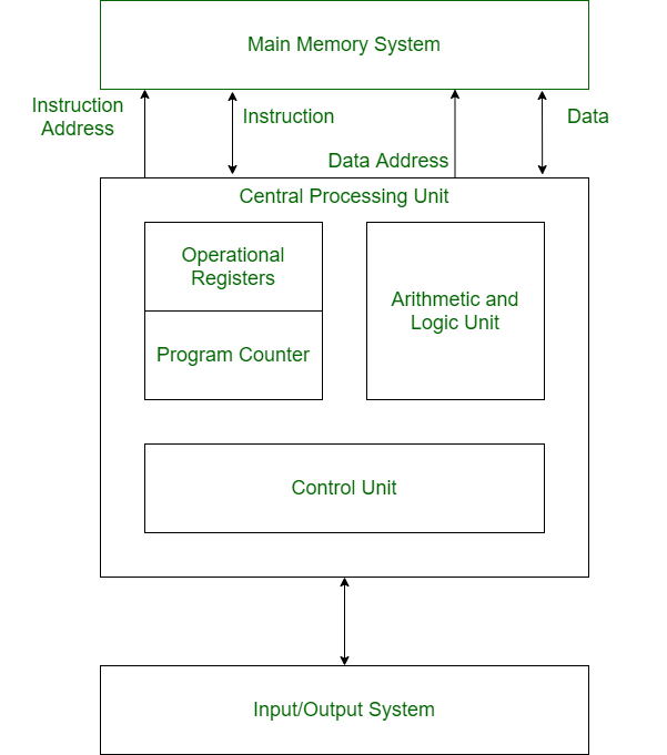
The basic Components of a Microprocessor-based system are as follows:
CPU Registers:
In computer architecture, a processor register is a very fast computer memory used to speed the execution of computer programs by providing quick access to commonly use values-typically, the values being in the midst of a calculation at a given point in time.
These registers are at the top of the memory hierarchy and are the fastest way for the system to manipulate data. A very simple microprocessor, it consists of a single memory location, usually called an accumulator. Registers are built from a fast multi-ported memory cell. They must be able to drive their data onto an internal bus in a single clock cycle. The result of the ALU operation is stored here and could be re-used in a subsequent operation or saved into memory. Registers are normally measured by the number of bits they can hold, for example, an “8-bit register” or a “32-bit register”. Registers are now usually implemented as a register file, but they have also been implemented using individual flip-flops, high-speed core memory, thin-film memory, and other ways in various machines.
There are several other classes of registers:
System Bus
The system bus is a cable that carries data communication between the major components of the computer, including the microprocessor. Not all of the communication that uses the bus involves the CPU, although naturally, the examples used in this tutorial will center on such instances. The system bus consists of three different groups of wiring, called the data bus, control bus, and address bus. These all have separate responsibilities and characteristics, which can be outlined as follows:
Control Bus
The control bus carries the signals relating to the control and coordination of the various activities across the computer, which can be sent from the control unit within the CPU. Different architectures result in a differing number of lines of wire within the control bus, as each line is used to perform a specific task. For instance, different, specific lines are used for each of reading, write and reset requests.
Data Bus
This is used for the exchange of data between the processor, memory and peripherals, and is bi-directional so that it allows data flow in both directions along the wires. Again, the number of wires used in the data bus (sometimes known as the 'width') can differ. Each wire is used for the transfer of signals corresponding to a single bit of binary data. As such, a greater width allows greater amounts of data to
be transferred at the same time.
Address Bus
The address bus contains the connections between the microprocessor and memory/IO devices that carry the signals relating to the addresses which the CPU is processing at that time, such as the locations that the CPU is reading from or writing to. The width of the address bus corresponds to the maximum addressing capacity of the bus or the largest address within memory that the bus can work with. The
addresses are transferred in binary format, with each line of the address bus carrying a single binary digit. Therefore the maximum address capacity is equal to two to the power of the number of lines present (2^n lines).